


IBM has unveiled the world’s first sub-1 nanometer chip. The new technology packs nearly 100 billion transistors onto a piece of silicon the size of a fingernail. A transistor architecture called “nanostack” makes it possible. The 3D design vertically stacks and staggers transistors. That pushes chip features past the 1 nm barrier and into the realm of individual atoms.
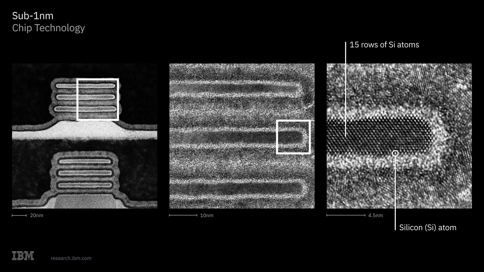
The chip operates at the 0.7 nm node, also called 7 angstrom. That means the transistor features are smaller than the width of a DNA strand, which measures about 2.5 nanometers. IBM says the design nearly doubles the transistor density of its 2 nm chip from 2021.
Published technical results point to major gains. The sub-1 nm chip could deliver up to 50 percent more performance. It could also achieve 70 percent better energy efficiency than IBM’s 2 nm node. Those gains could supercharge compute-heavy workloads like generative AI and cloud infrastructure.
“With our new nanostack architecture, we’re not just making smaller transistors,” said Jay Gambetta, director of IBM Research. “We’re reinventing how chips are built to deliver dramatically more power and energy efficiency.”
How nanostack works
The nanostack architecture breaks from conventional chip design. Instead of laying transistors flat, IBM researchers glue together two wafers with nanosheet-style transistors. They stack them vertically like a sandwich. The 3D approach lets each layer use different material combinations. That optimizes performance and power efficiency for individual transistors.
IBM validated the design through several tests. These included ultra-thin dielectric bonding and functional CMOS inverter operation with expected switching performance. At VLSI 2026, the company also showed that nanostack delivers 40 percent scaling in SRAM. That lets chip designers build more efficient processors for advanced AI workloads.
Beyond Moore’s Law
The announcement comes as the semiconductor industry grapples with the apparent end of Moore’s Law. Intel co-founder Gordon Moore observed that transistor counts double roughly every two years. But as transistors shrink toward atomic dimensions, the physics gets harder. Scaling has slowed considerably since around 2016.
“I’ve spent over 20 years in the semiconductor industry at IBM,” said Huiming Bu, vice president of IBM’s silicon technology research team. “We’ve heard many times that scaling is reaching its limits. What we’ve learned is that progress doesn’t stop. It just requires a new paradigm.”
IBM and partners like Lam Research, Tokyo Electron, and SCREEN Semiconductor Solutions conduct this work in Albany, New York. The facility will soon add a High NA EUV lithography tool from ASML. That equipment prints ultra-precise circuits essential for pushing chips even smaller.
Don’t expect nanostack chips in consumer devices soon. IBM pegs the earliest production path at roughly five years. Researchers still face challenges like thermal management and integration with existing systems. But IBM’s roadmap now projects at least a decade of continued scaling. The company is betting the atomic era of chipmaking has only just begun.


